- 您现在的位置:买卖IC网 > Sheet目录3881 > PIC18F6525T-I/PT (Microchip Technology)IC PIC MCU FLASH 24KX16 64TQFP
PIC18F6525/6621/8525/8621
DS39612B-page 120
2005 Microchip Technology Inc.
10.7
PORTG, TRISG and LATG
Registers
PORTG is a 6-bit wide port with 5 bidirectional pins
(RG0:RG4) and one optional input only pin (RG5). The
corresponding data direction register is TRISG. Setting
a TRISG bit (= 1) will make the corresponding PORTG
pin an input (i.e., put the corresponding output driver in
a high-impedance mode). Clearing a TRISG bit (= 0)
will make the corresponding PORTC pin an output (i.e.,
put the contents of the output latch on the selected pin).
The Data Latch register (LATG) is also memory
mapped. Read-modify-write operations on the LATG
register, read and write the latched output value for
PORTG.
PORTG is multiplexed with both CCP/ECCP and
EUSART functions (Table 10-13). PORTG pins have
Schmitt Trigger input buffers.
When enabling peripheral functions, care should be
taken in defining TRIS bits for each PORTG pin. Some
peripherals override the TRIS bit to make a pin an
output, while other peripherals override the TRIS bit to
make a pin an input. The user should refer to the
corresponding peripheral section for the correct TRIS
bit settings.
The pin override value is not loaded into the TRIS reg-
ister. This allows read-modify-write operations of the
TRIS register without concern due to peripheral
overrides.
The sixth pin of PORTG (MCLR/VPP/RG5) is a digital
input pin. Its operation is controlled by the MCLRE
configuration
bit
in
Configuration
Register
3H
(CONFIG3H<7>).
In
its
default
configuration
(MCLRE = 1), the pin functions as the device Master
Clear input. When selected as a port pin (MCLRE = 0),
it functions as an input only pin; as such, it does not
have TRISG or LATG bits associated with it.
In either configuration, RG5 also functions as the
programming voltage input during device programming.
EXAMPLE 10-7:
INITIALIZING PORTG
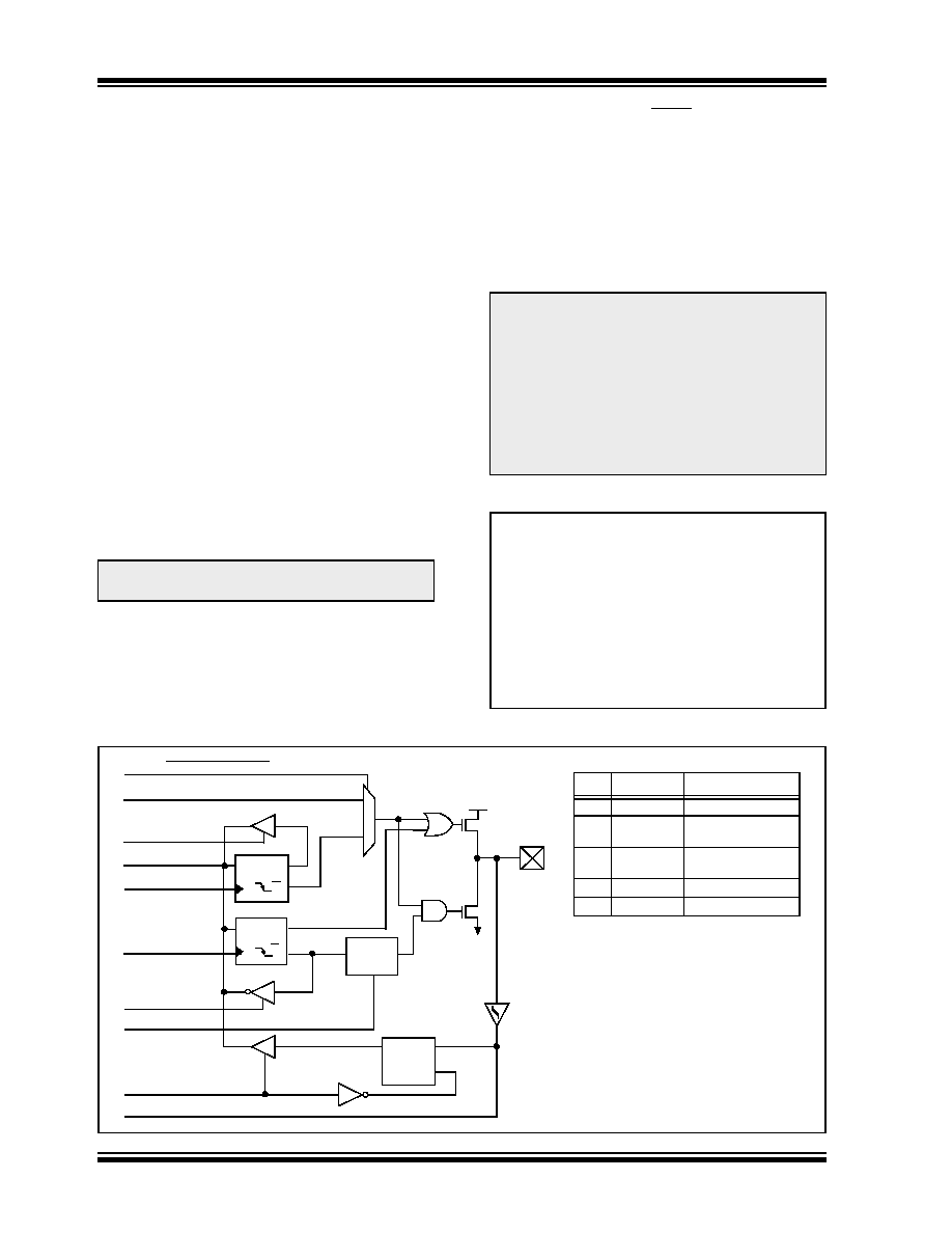
FIGURE 10-16:
PORTG BLOCK DIAGRAM (PERIPHERAL OUTPUT OVERRIDE)
Note:
On a Power-on Reset, these pins are
configured as digital inputs.
Note 1: On a Power-on Reset, RG5 is enabled as
a digital input only if Master Clear
functionality is disabled (MCLRE = 0).
2: If the device Master Clear is disabled,
verify that either of the following is done to
ensure proper entry into ICSP mode:
a.) disable low-voltage programming
(CONFIG4L<2> = 0); or
b.) make certain that RB5/KBI1/PGM is
held low during entry into ICSP.
CLRF
PORTG
; Initialize PORTG by
; clearing output
; data latches
CLRF
LATG
; Alternate method
; to clear output
; data latches
MOVLW
0x04
; Value used to
; initialize data
; direction
MOVWF
TRISG
; Set RG1:RG0 as outputs
; RG2 as input
; RG4:RG3 as inputs
PORTG/Peripheral Out Select
Data Bus
WR LATG
WR TRISG
Data Latch
TRIS Latch
RD TRISG
Q
D
Q
CK
QD
EN
Peripheral Data Out
0
1
Q
D
Q
CK
P
N
VDD
VSS
RD PORTG
Peripheral Data In
I/O pin(1)
or
WR PORTG
RD LATG
Schmitt
Trigger
TRIS
Override
Peripheral Output
Logic
TRIS OVERRIDE
Pin
Override
Peripheral
RG0
Yes
ECCP3 I/O
RG1
Yes
USART1 Async Xmit,
Sync Clock
RG2
Yes
USART1 Async Rcv,
Sync Data Out
RG3
Yes
CCP4 I/O
RG4
Yes
CCP5 I/O
Enable(2)
Note 1: I/O pins have diode protection to VDD
and VSS.
2: Peripheral output enable is only active
if peripheral select is active.
发布紧急采购,3分钟左右您将得到回复。
相关PDF资料
PIC18F4439-E/ML
IC PIC MCU FLASH 6KX16 44QFN
XF2J-2024-11
CONN FPC 20POS 0.5MM SMT
PIC16LF747-I/ML
IC PIC MCU FLASH 4KX14 44QFN
XF2J-1824-11
CONN FPC 18POS 0.5MM SMT
XF2J-1624-11
CONN FPC 16POS 0.5MM SMT
XF2J-1424-11
CONN FPC 14POS 0.5MM SMT
XF2J-1224-11
CONN FPC 12POS 0.5MM SMT
XF2J-1024-11
CONN FPC 10POS 0.5MM SMT
相关代理商/技术参数
PIC18F6527-I/PT
功能描述:8位微控制器 -MCU 48 KB FL 4K RAM 70 I/O RoHS:否 制造商:Silicon Labs 核心:8051 处理器系列:C8051F39x 数据总线宽度:8 bit 最大时钟频率:50 MHz 程序存储器大小:16 KB 数据 RAM 大小:1 KB 片上 ADC:Yes 工作电源电压:1.8 V to 3.6 V 工作温度范围:- 40 C to + 105 C 封装 / 箱体:QFN-20 安装风格:SMD/SMT
PIC18F6527-I/PT
制造商:Microchip Technology Inc 功能描述:8-Bit Microcontroller IC
PIC18F6527T-I/PT
功能描述:8位微控制器 -MCU 48 KB FL 4K RAM 70 I/O RoHS:否 制造商:Silicon Labs 核心:8051 处理器系列:C8051F39x 数据总线宽度:8 bit 最大时钟频率:50 MHz 程序存储器大小:16 KB 数据 RAM 大小:1 KB 片上 ADC:Yes 工作电源电压:1.8 V to 3.6 V 工作温度范围:- 40 C to + 105 C 封装 / 箱体:QFN-20 安装风格:SMD/SMT
PIC18F6585-E/L
功能描述:8位微控制器 -MCU 48KB 3328 RAM 52 I/O RoHS:否 制造商:Silicon Labs 核心:8051 处理器系列:C8051F39x 数据总线宽度:8 bit 最大时钟频率:50 MHz 程序存储器大小:16 KB 数据 RAM 大小:1 KB 片上 ADC:Yes 工作电源电压:1.8 V to 3.6 V 工作温度范围:- 40 C to + 105 C 封装 / 箱体:QFN-20 安装风格:SMD/SMT
PIC18F6585-E/PT
功能描述:8位微控制器 -MCU 48KB 3328 RAM 52 I/O RoHS:否 制造商:Silicon Labs 核心:8051 处理器系列:C8051F39x 数据总线宽度:8 bit 最大时钟频率:50 MHz 程序存储器大小:16 KB 数据 RAM 大小:1 KB 片上 ADC:Yes 工作电源电压:1.8 V to 3.6 V 工作温度范围:- 40 C to + 105 C 封装 / 箱体:QFN-20 安装风格:SMD/SMT
PIC18F6585-I/L
功能描述:8位微控制器 -MCU 48KB 3328 RAM 52 I/O RoHS:否 制造商:Silicon Labs 核心:8051 处理器系列:C8051F39x 数据总线宽度:8 bit 最大时钟频率:50 MHz 程序存储器大小:16 KB 数据 RAM 大小:1 KB 片上 ADC:Yes 工作电源电压:1.8 V to 3.6 V 工作温度范围:- 40 C to + 105 C 封装 / 箱体:QFN-20 安装风格:SMD/SMT
PIC18F6585-I/L
制造商:Microchip Technology Inc 功能描述:8-Bit Microcontroller IC
PIC18F6585-I/PT
功能描述:8位微控制器 -MCU 48KB 3328 RAM 52 I/O RoHS:否 制造商:Silicon Labs 核心:8051 处理器系列:C8051F39x 数据总线宽度:8 bit 最大时钟频率:50 MHz 程序存储器大小:16 KB 数据 RAM 大小:1 KB 片上 ADC:Yes 工作电源电压:1.8 V to 3.6 V 工作温度范围:- 40 C to + 105 C 封装 / 箱体:QFN-20 安装风格:SMD/SMT